For decades, scientists were baffled by the behavior of semiconductors. For example, in early 1940 a Bell Labs scientist names Russell S. Ohl fashioned a block of silicon that was divided into two different electrical regions, one containing an excess of electrons and another an excess of holes, or positive charges. (This was accomplished by doping, or chemically contaminating, the silicon with positive and negative impurities during manufacture.) Much to his astonishment, Ohl discovered that the silicon generated half a volt of electricity when a light was shined on the dividing line between the positive and negative zones, or the pn junction. In other words, the silicon converted light into power. Scientists had been aware of the photoelectric properties of semiconductors since the 1920s, but no semiconductor had ever produced so much electricity. Clearly, something unusual was taking place at the pn junction.
In July 1945, a month before the end of the war, Bell Labs decided to set up a larger research program on solid-state physics. The phone company used tubes and mechanical relays by the millions, but the tubes eventually burned out and the relays, being mechanical, occasionally malfunctioned – and the company dreamed of replacing all these parts with uncomplaining solid-state components. As part of the research effort, Bell assigned a small group to study semiconductors. Made up mostly of theoretical physicists, the group was headed by William Shockley, a physicist with a brilliant talent for devising experiments that went to the heart of a matter. The team also included the physicists John Bardeen and Walter Brattain. Bardeen, the youngest of the three, had joined Bell only recently, and had never worked on semiconductors, but Shockley and Brattain, who had both been at the labs for years, had a long-standing interest in solid-state physics; in fact, Brattain had seen Ohl ‘s miraculous block of silicon at work, an experience he never forgot.
The men decided to focus on silicon and germanium, the simplest semiconductors, and to try to understand the nature of the pn junction. As Brattain recalled, the group was quite close knit:
I cannot overemphasize the rapport of this group. We would meet together to discuss important steps almost on the moment of an afternoon. We would discuss things freely, one person’s remark s suggesting an idea to another. We went to the heart of many things during the existence of this group and always when we got to the place where something had to be done, experimental or theoretical, there never was any question as to who was the appropriate man in the group to do it.
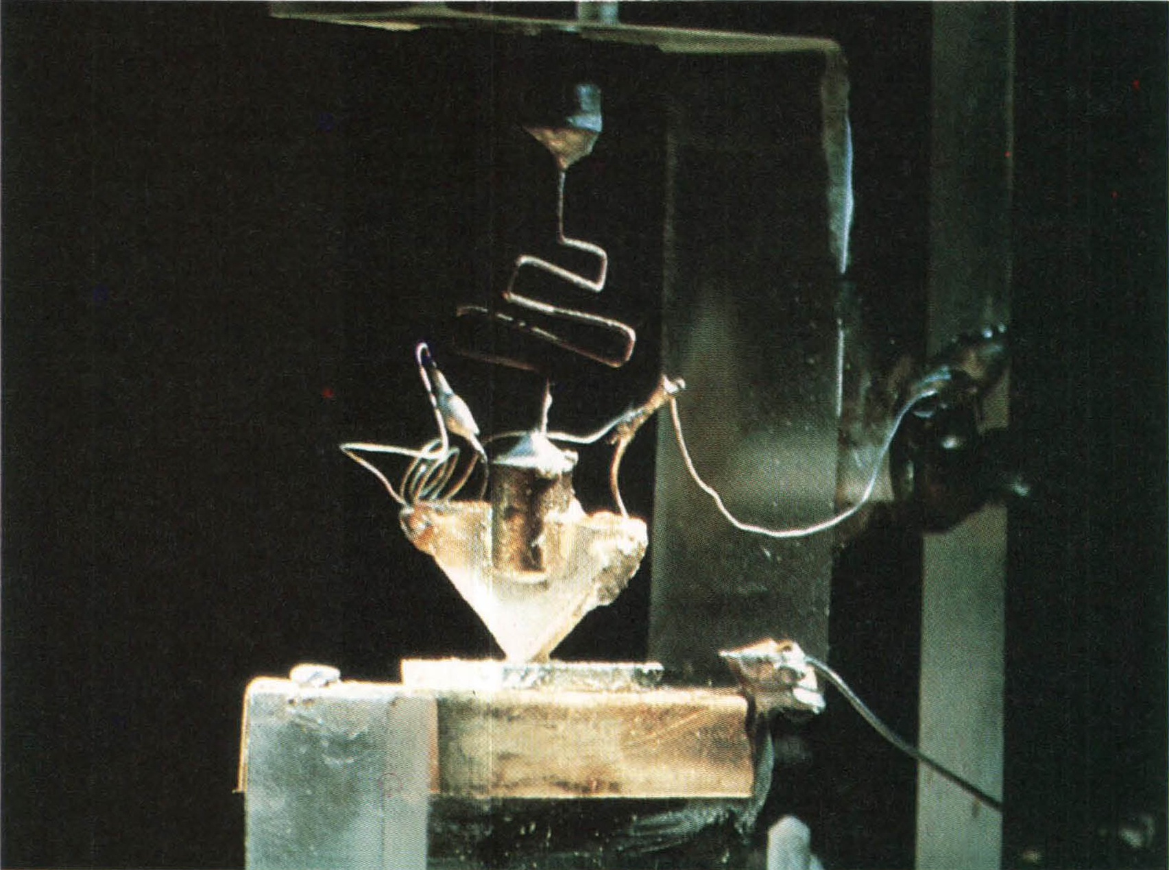
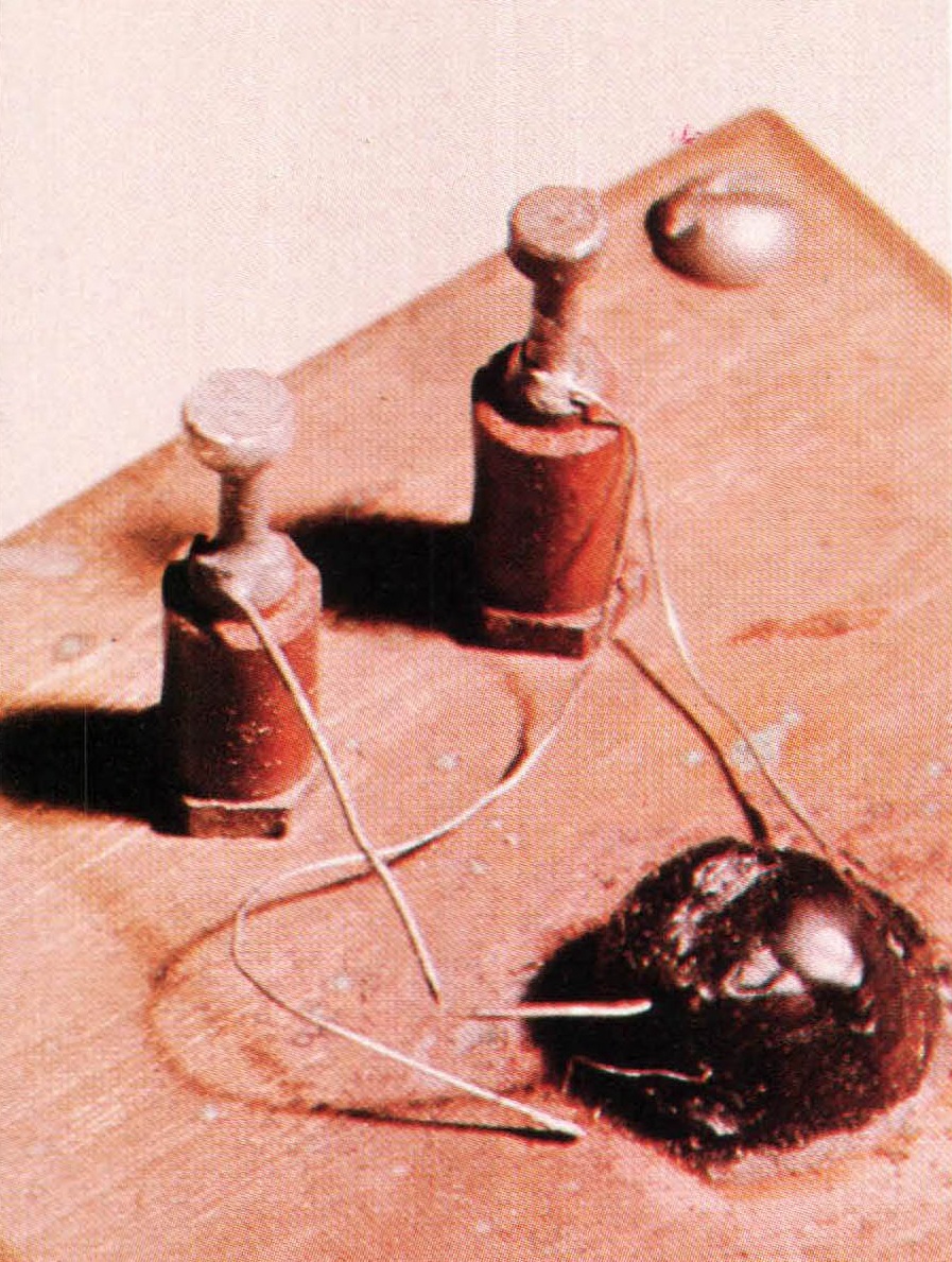
Success came fairly quickly. At the end of December 1947, after two frustrating but exhilarating years of work, Bardeen and Brattain managed to create an amplifying circuit based on a small slab of germanium with two pn junctions. “This circuit was actually spoken over,” Brattain wrote in his lab notebook on December 24, the day after the first demonstration, “and by switching the device in and out, a distinct gain in speech level could be heard and seen on the scope presentation with no noticeable change in quality. … It was determined that the power gain was on the order of a factor of 18 or greater.”
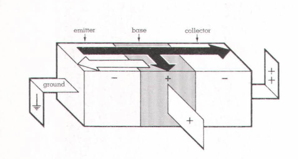
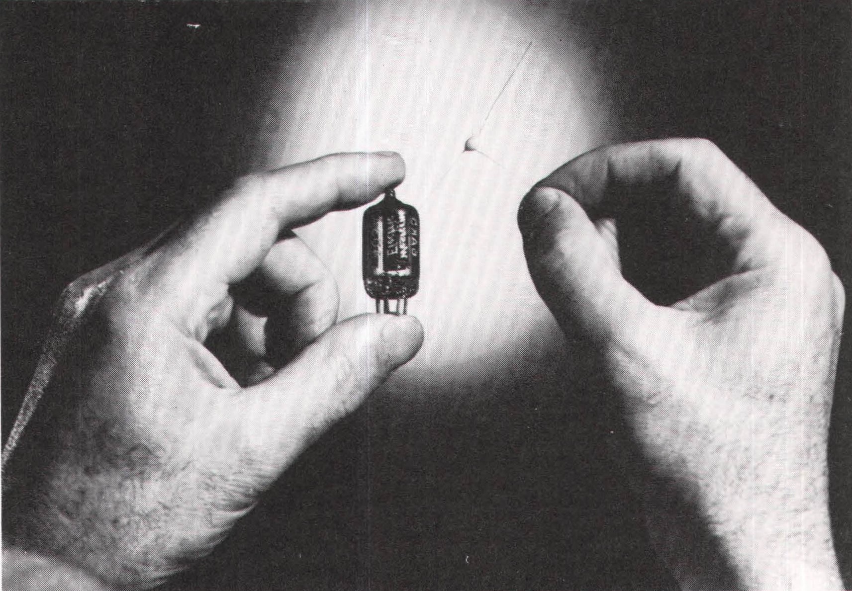
Called the point-contact transistor, Bardeen and Brattain’s invention proved to be very difficult to manufacture. In 1951, Shockley developed an improved version, the junction, or bipolar, transistor, and the transistor moved from the laboratory to the factory. Both devices operate like the triode. But instead of a cathode and anode, a transistor has an emitter and a collector. And instead of a grid, it has a base. Unlike the parts of a triode, however, these components are intrinsic parts of the transistor – there are no glass tubes or metal grids here. Essentially, a transistor is an electrical sandwich consisting of two pn junctions, one between the emitter and the base, another between the base and the collector. The emitter and the collector – the bread of the sandwich carry a negative polarity, whereas the base – the meat of the sandwich – bears a positive charge. (In some transistors, the polarity of the components is the other way around, or positive-negative- positive.) When a voltage is applied to the base, electrons surge from the emitter across the base to the collector, amplifying the current.
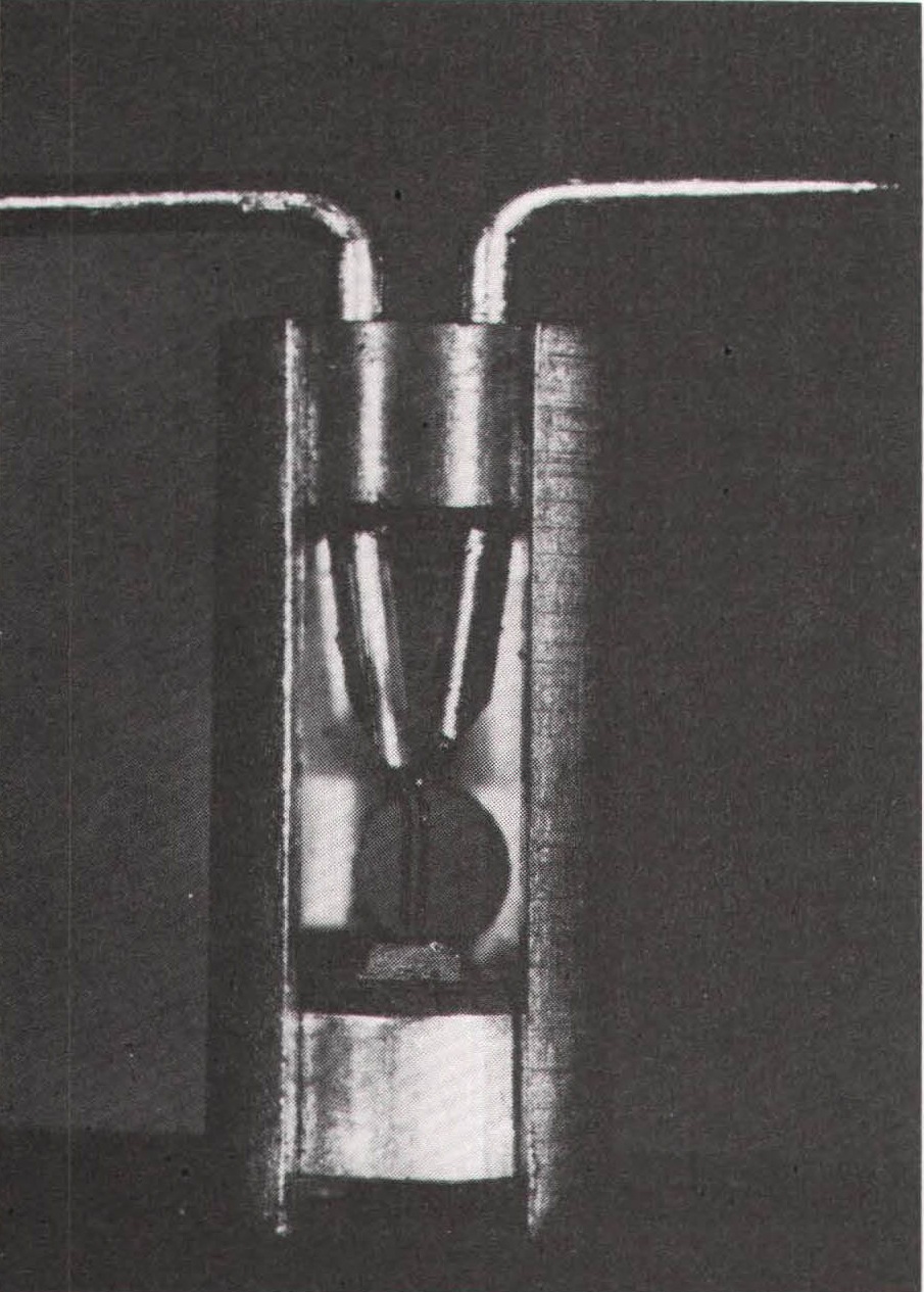
Introduced to the public at a news conference in Manhattan in July 1948, the point-contact transistor attracted a modest amount of attention. In general, it was regarded as a novelty dreamed up by the phone company, and it wasn’t until the early 1950s, with the advent of Shockley’s junction transistor, that the importance of the device sunk in. Bell Labs was willing to license the rights to the transistor to any company in exchange for a royalty (with the exception of hearing aid manufacturers, which Bell exempted from paying royalties, as a gesture in memory of Alexander Graham Bell). In 1952, Bell Labs held a course on transistor technology for its licensees. Just as the Moore School’s famous class on computers disseminated the technology of ENIAC and EDVAC, Bell Labs’ symposium disseminated transistor technology to the electronics industry. Transistors first reached the public in 1953 as amplifiers in hearing aids, and transistor radios came along the following year.
Naturally, computer manufacturers were keenly interested in the device. In February 1956, the scientists in MIT’s Digital Computer Lab, working with IBM, started developing a transistorized computer to replace the massive vacuum-tube machines of SAGE. Although the MIT-IBM machine worked well, the 55,000 tube SAGE computers were already in production; since millions of dollars had been spent on the tube machines, the Air Force saw no reason to replace them. Meanwhile, the computer industry began designing transistorized computers for the commercial market. The first ones appeared in 1957 and 1958, introduced by UNIVAC and the Philco Corporation. Compared to their be-tubed predecessors, the new generation of computers was superior in every way – smaller, faster, more reliable and economical, and much more powerful.
