The son of a Congregationalist minister, Noyce grew up in Grinnell, Iowa, an ordinary Midwestern town with a population of 7,000 in 1948. As a physics major at Grinnell College, he was introduced to solid-state physics by Grant Gale, the school’s physics professor and a friend of John Bardeen’s. In the summer of 1948, Gale read a little item in the newspaper about the invention of the transistor, and he asked Bardeen to send him some samples for his students. Noyce was one of the first people in the country to experiment with a transistor, and he decided to specialize in solid-state physics at graduate school. He went to MIT, where, much to his surprise, few people had even heard about the transistor, let alone experimented with one. There weren’t any courses in solid-state physics, at MIT or any other school- and there wouldn’t be until the mid-1950s. Gale was one of the few professors who knew anything about transistor electronics, and he and Noyce often compared notes. When Noyce received his Ph.D. in 1953, he headed straight for industry, where most solid-state research was being conducted. His first job was with Philco, in Philadelphia, which he chose because the company was opening a semiconductor operation and the chances for advancement seemed best there. But it turned out that Philco wasn’t really interested in advanced research, and Noyce soon began to look elsewhere.
In 1955, he and a Swiss-born physicist named Jean Hoerni arrived in Mountain View, California, to go to work for Shockley Semiconductor Laboratory, a small company that William Shockley, the transistor’s co-inventor, had set up in the hope of cashing in on his knowledge of solid-state physics. (Mountain View is next door to Palo Alto, Shockley’s hometown and the home of Stanford University.) Shockley Semiconductor Laboratory, begun with support from Arnold Beckman of Beckman Instruments, was an unprepossessing outfit; it occupied a glorified shed on South San Antonio Road and had about fifteen employees.
Although Shockley was a brilliant research director, with an uncanny sense for the experimental jugular, he was a poor manager of people and money and held a somewhat conspiratorial view of the world. He posted a list of everyone’s salaries, hoping to put an end to company secrets; he required his employees to rate one another regularly, a process that immediately degenerated into a popularity contest; and, after the lab ‘s work ran into in explicable delays which Shockley unaccountably blamed on sabotage, he ordered one of his employees to take a lie detector test. (The man passed.) Moreover, for all his technical brilliance, he insisted on concentrating on a device known as a four-layer germanium diode (a switch with a very strong off state and a correspondingly weak on state), which had only a wisp of a chance at commercial success. Noyce, Hoerni, and most of their colleagues believed that they ought to be working on silicon transistors, which had much greater commercial promise.

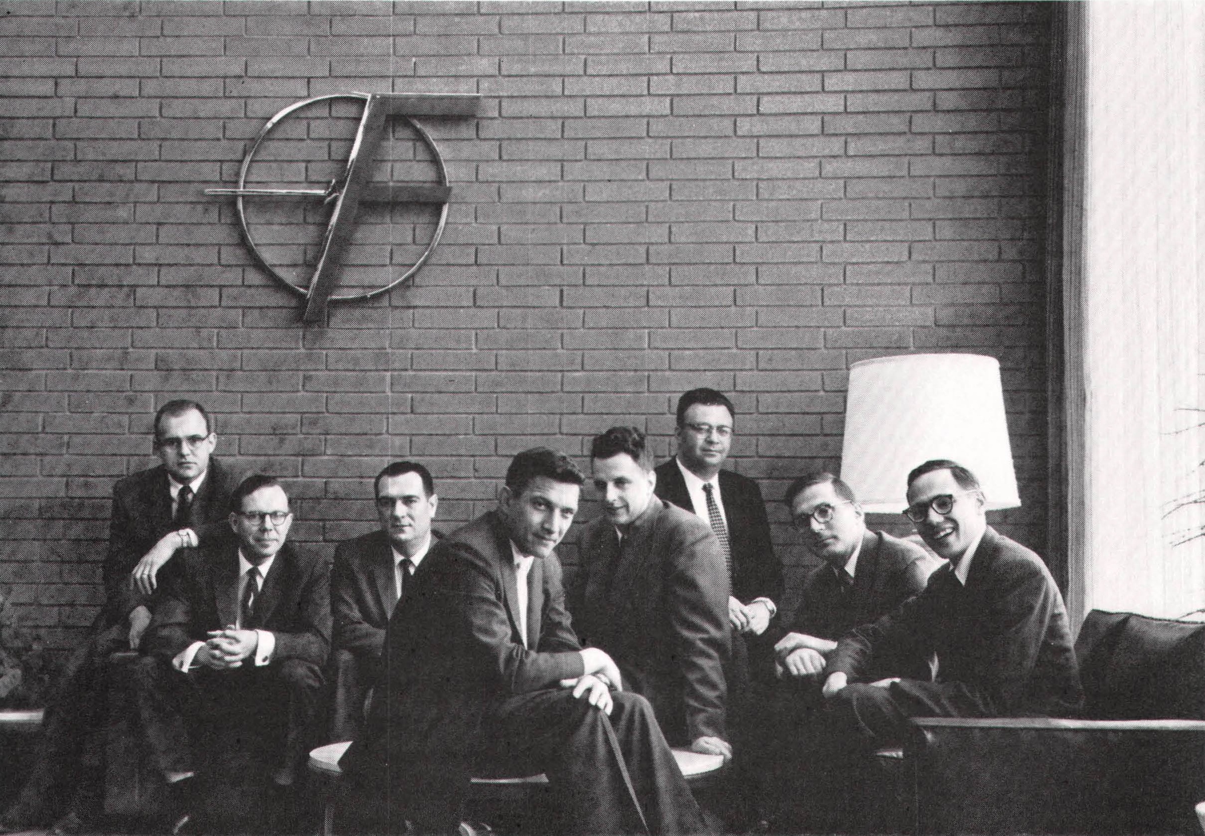
By the summer of 1957, Noyce, Hoerni, and six other scientists and engineers at the lab had had enough. Realizing that brainpower constituted the real assets of a semiconductor firm, they decided to go into business for themselves. The Fairchild Camera & Instrument Corporation of New York agreed to finance them, and Fairchild Semiconductor was born, moving into a large garage in Palo Alto while their new two-story concrete building, near the Shockley lab, was being completed. Although Fairchild’s founders had an equal say in the direction of the enterprise, Noyce’s confident, relaxed manner made him the most popular member of the group, and he became the company’s general manager. At that time, Fairchild and Shockley were the only semiconductor operations in the Santa Clara Valley, a sunny region of fruit farms about fifty miles south of San Francisco, now popularly known as Silicon Valley. A few large companies, such as IBM and General Electric, had divisions there, along with Hewlett-Packard, Raytheon Associates, and other homegrown outfits established by former Stanford students. The university encouraged graduates to set up companies in the area, offering them inexpensive, longterm leases on Stanford land.
Unlike Shockley’s outfit, Fairchild Semiconductor concentrated on silicon transistors. In the late 1950s, the state of the art in transistors was the silicon mesa transistor (which had been invented by Bell Labs and which Jack Kilby had used in his ICs). It consisted of a tiny round plateau, or mesa, set above a surrounding base of silicon; a semicircular ring on top of the mesa served as the emitter, the transistor’s controlling component, with the surrounding plane acting as the collector. Mesa transistors, which were made through photolithography, etching, and diffusion (chemically doping the semiconductor with impurities), seemed to have a great deal of promise; but a significant drawback soon appeared. Since the mesas protruded from the wafers, the transistors were subject to contamination of all kinds, and the connecting wires tended to slip. You sometimes could short-circuit a mesa transistor merely by tapping on its container.

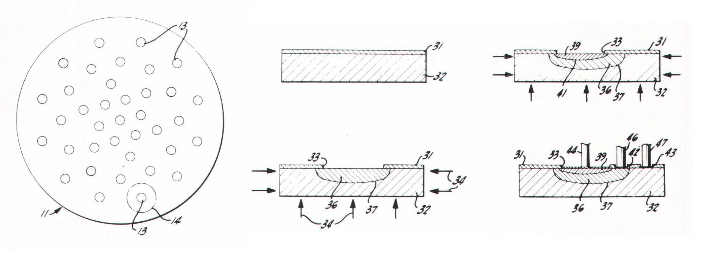
In late 1958 and early 1959, Jean Hoerni came up with a brilliant solution to the mesa’s problems. He diffused the mesa into the wafer; in other words, he chemically embedded the transistor’s various parts into a piece of silicon. (See the illustration on page 241.) The result was a completely flat transistor, one without any protruding parts. Then he coated the gadget with a thin layer of silicon dioxide, which insulated, or protected, the transistor much as rubber insulates wire. However, he coated the device in such a way that certain spots were left uncovered, creating convenient contact points for the wires. Although the wires jutted out, just as they did on the mesa transistor, Hoerni’s device was much better protected from contamination and slipped wires, and it was, therefore, much more reliable. Hoerni’s planar process was a great technical breakthrough, and it led directly to the invention of a commercially feasible IC.
By early 1959, only one other piece was missing from the IC puzzle, and it was supplied by the Sprague Electric Company in North Adams, Massachusetts. The company’s research director, Kurt Lehovec, a Czech-born physicist who had immigrated to the United States after World War II, had been working on better ways to make alloy junction transistors (an advanced form of the transistor Shockley had invented). Lehovec devised an improved manufacturing process and that success inspired him to ponder the problem of how to build an IC – of how to isolate the components electrically. His solution was similar to one of Kilby’s: pn junctions, which allow electricity to flow in one direction only.

“The idea was shamelessly simple,” said Lehovec, now an engineering professor at the University of Southern California, “and I realized that it was important to file a patent on it immediately.” He had heard about Kilby’s work – and he had surmised that the Texan’s devices didn’t incorporate pn junctions. (They did, but Kilby had made poor use of them.) Lehovec designed an IC whose components were separated by pn junctions, and filed a patent application on 22 April 1959, six weeks after TI had gone public with Kilby’s invention. Lehovec’s IC wasn’t much better than Kilby’s, but he had hit upon the best way to isolate the components.
Meanwhile, Noyce also was thinking about how to make an IC. In January 1959 – about a year after Hoerni had developed the planar process and about four months after Kilby had fashioned his first solid circuit – Noyce made his first notes on the subject in his lab journal. Six months later, he succeeded in developing an IC based on Hoerni’s planar process and Lehovec’s pn junctions. As he recalled years later:
When this [the planar process] was accomplished, we had a silicon surface covered with one of the best insulators known to man, so you could etch holes through to make contact with the underlying silicon. Obviously, then, you had a whole bunch of transistors embedded in an insulating surface, and the next thing was that, instead of cutting them apart physically, you cut them apart electrically, added the other components you needed for circuits, and finally the interconnection wiring.
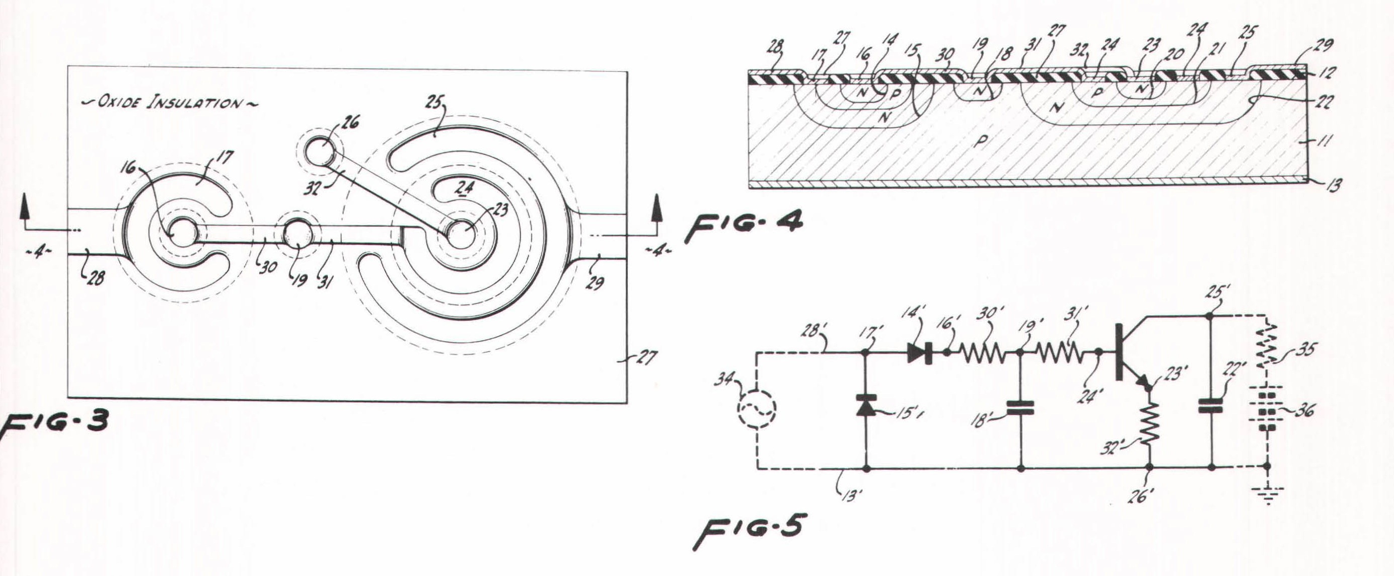
There were several techniques, but the main one was, basically, to build back-to-hack diodes [or pn junctions] into the silicon between any two transistors so that no current could flow between the two in either direction. The other element you needed was a resistor, and it was relatively simple to make a diode-isolated piece of silicon that acts as a resistor. You now had resistors and transistors, and could start building logic circuits, which you could interconnect by evaporating metal on top of the insulating layer. [That was one of Noyce’s key innovations. By evaporating the connections onto the chip through a mask, he kept the IC flat.] So it was a progressive buildup of bits and pieces of the technology to make the entire thing possible.
It was a question of having these rather vague concepts of insulators, of isolation, of interconnection, and the photoengraving for the patterns, so that you drew on your bag of tricks to combine these elements to make the integrated circuit. There was no huge flashbulb flashing, but it was almost as if you sat down as a semiconductor physicist and asked, “How can I do this job?” There is no doubt in my mind that if the invention hadn’t arisen at Fairchild, it would have arisen elsewhere in the very near future. It was an idea whose time had come, where the technology had developed to the point where it was viable.

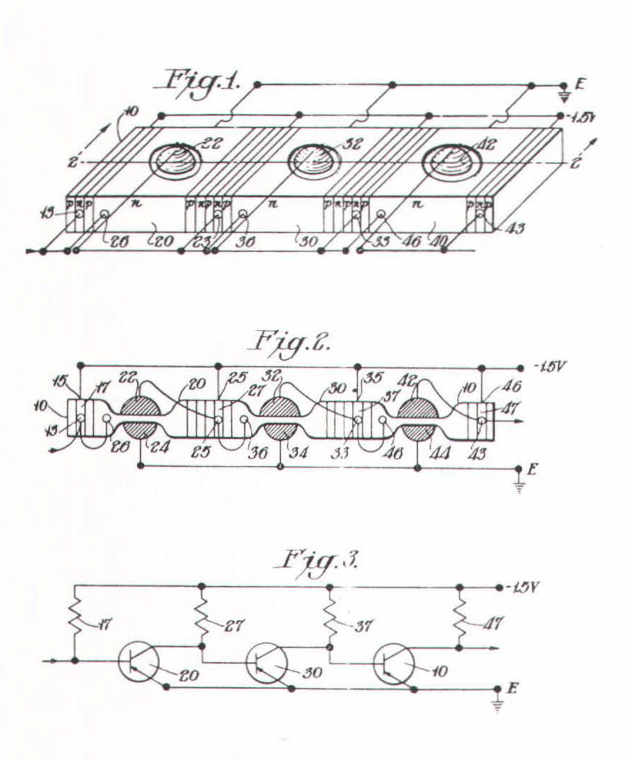
Noyce’s IC was an elegant little device. Based on the planar process, it had no protruding parts. Instead of vertical contact wires, it used horizontal ones, snaking around the face of the chip. And instead of isolating components by shaping the chip, it used pn junctions. Above all, it lent itself to mass production and almost unlimited refinement. Noyce’s IC was the right approach.