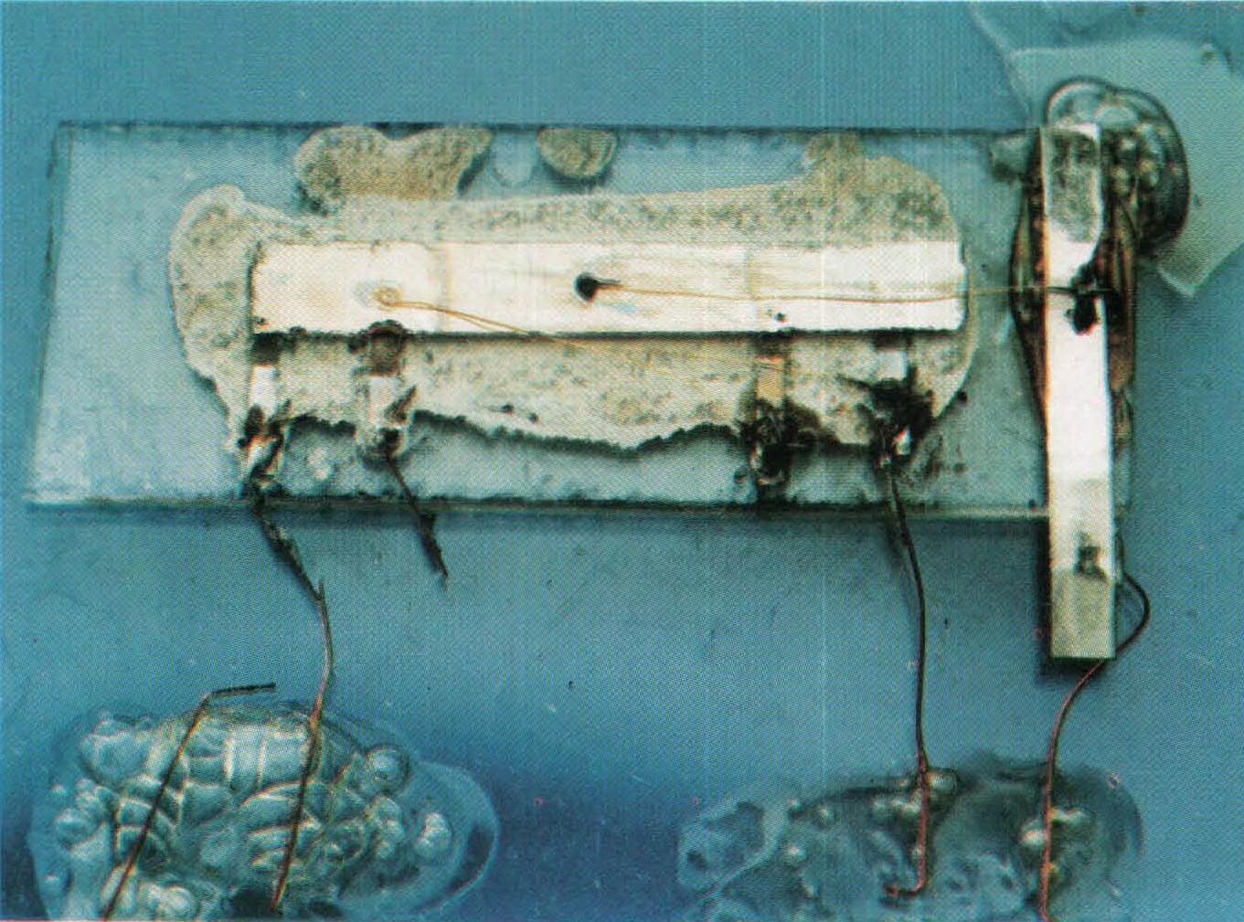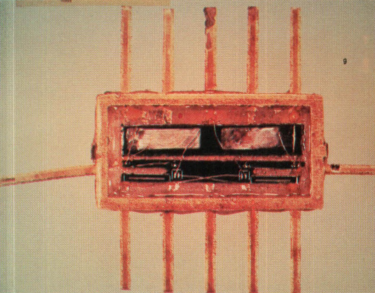
The demonstration was easy enough; Kilby pulled some silicon transistors and unprocessed silicon wafers off TI’s shelves, modified them, and constructed a discrete flip-flop. Making a solid circuit was a much more difficult matter, but Kilby drew on a deeper well of ingenuity and, with the help of two technicians, managed to fashion a simplified phase-shift oscillator out of a germanium wafer. This circuit was built in a hurry and was every bit as crude looking as the first transistor; Kilby was well aware of the importance of his idea and didn’t want to lose the race to another company. He tested the gadget on 12 September 1959, and it worked.

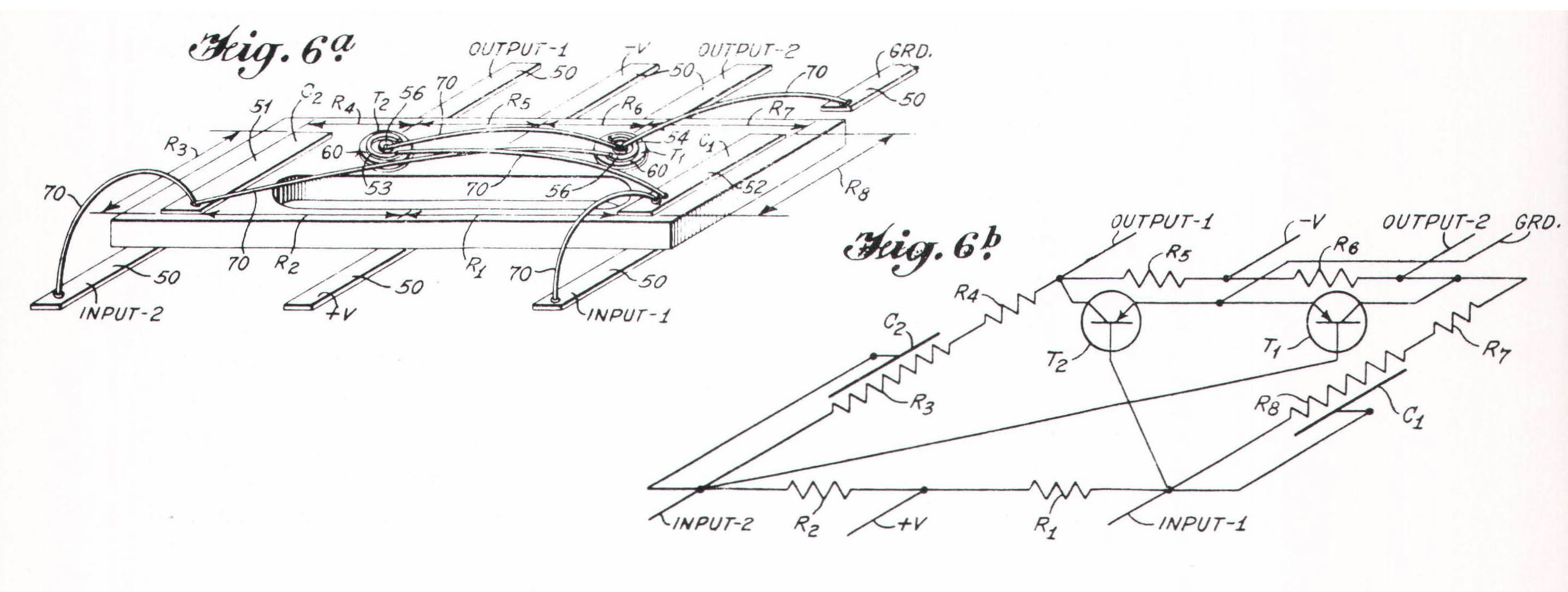
Kilby constructed other solid circuits during the next few months, including a flip-flop. It is the best illustration of Kilby’s techniques, showing both the cleverness of his conception and the nature of its shortcomings, and it’s worth a close examination. (A drawing of the circuit, reproduced from Kilby’s patent, is at left.) In considering this IC, it’s important to keep three questions in mind. How did Kilby isolate the IC’s components electrically, so that the operation of one part wouldn’t interfere with the workings of another? How did he manage to fashion passive devices, such as capacitors and resistors, out of a semiconductor? And how did he wire up the IC’s various components? These are the same questions that Dummer and other would-be inventors of the IC had to face, and the value of their achievements rose or fell according to how well they answered them.
In brief, and without getting too technical, we can say that Kilby wired up the IC as though it were an ordinary component – that is, simply by soldering tiny wires to the various parts of the circuit. The more complicated the circuit, the more wires it had. And every one had to be affixed by hand, using tweezers and a microscope. If the wires weren’t soldered on solidly and firmly, they could be dislodged by vibration and shock. (Not all electronic components go into stereos and TV sets; they are also used in missiles and tanks.) As long as the IC wasn’t too small or complicated, the wiring process wasn’t too difficult, but the wiring requirement of Kilby’s ICs limited the potential sophistication of the devices. It would be impossible to make a Kilby-style IC containing, say, 10,000 components.

As for the second question, how to create passive devices out of a semiconductor, Kilby came up with an ingenious answer. The IC has two capacitors (the narrow raised strips on either side of the device, labeled C1 and C2) and eight resistors (intrinsic parts of the device, labeled R1 to R8). The capacitors were created by coating a section of the IC with a thin layer of silicon dioxide, an insulator, and then placing a thin strip of gold or aluminum over the oxide. The result is a very simple capacitor; when a charge is dispatched to the capacitor, it is stored safely in the gold or aluminum strip, and the silicon dioxide prevents the electricity from leaking away and interfering with the other components.
The third and last problem, how to isolate the IC’s various components, was solved primarily by “shaping” the IC into L’s, U’s, and other configurations. “This shaping concept,” Kilby wrote in his patent application, “makes it possible in a circuit to obtain the necessary isolation between components and to define the components or, stated differently, to limit the area which is utilized for a given component.” Shaping was an inelegant solution to a complicated problem and, as we shall see, soon was superseded by a superior technique developed by another company. In addition to shaping, Kilby also isolated the IC’s components with resistors, sprinkled liberally around the device. The resistors were merely pn junctions, which permit electricity to flow in one direction only. (If a positive current surging through a negative zone suddenly came up against a positive area, it would be repelled, and vice versa. It’s an old principle: opposites attract, likes repel.) Unfortunately, pn junctions played a secondary role in Kilby’s ICs.

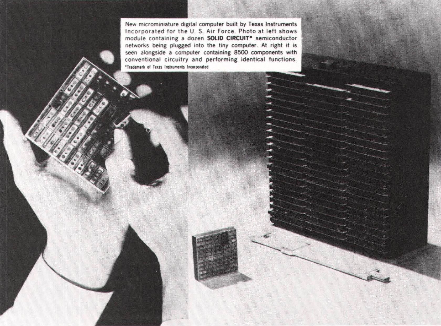
Compared to micromodules, Kilby’s ICs were a major step forward, “It is possible,” Kilby declared in his patent, “… to achieve component densities of greater than thirty million per cubic foot as compared with five hundred thousand per cubic foot , which is the highest component density attained prior to this invention.” In a vivid demonstration of the miniaturizing potential of ICs, TI built a tiny computer for the Aeronautical Systems Division of the Air Force. It contained 587 ICs, measured 6.3 cubic inches, weighed 10 ounces – and possessed the same computational power as a transistorized computer that had 8,500 components, occupied 1,000 cubic inches, and weighed 480 ounces. But the IC’s chips were unreliable and difficult to make, especially compared to the elegant and eminently practical IC developed by Robert Noyce at Fairchild.