
While the transistor was remaking computers, another technology, even more revolutionary, was beginning to take shape. One of the first people to point the way was an English engineer named G. W. A. Dummer. An expert in electronic reliability, Dummer worked for the Royal Radar Establishment, in Malvern, northern England, where he was in charge of a group that, among other things, developed electronic components hardy enough to withstand the effects of harsh climates. His group spent most of its time testing radar equipment, using such devices as centrifuges, refrigerators, atmospheric chambers, high-humidity tropical testing chambers, and so on. As tubes gave way to transistors and other semiconductors, radar equipment became smaller and more reliable. All things being equal, reliability and miniaturization were intertwined: the smaller the device, the fewer the parts and interconnections; the fewer the parts and interconnections, the higher the reliability.
The more Dummer considered the relation between reliability and miniaturization, the more it seemed to him that the key to the problem – how to make radar and other electronic equipment highly reliable – was miniaturization. At that time, electrical circuits consisted of various discrete components, each manufactured separately, packaged in its own container, and wired one at a time into a circuit board. Why not, Dummer asked, develop components that incorporated many transistors, capacitors (which store charges), resistors (which do just that), and other parts into the same solid, inseparable piece of material? For example, instead of inserting several transistors into a board, you’d use a single solid circuit composed of many transistors, thus cutting down on the number of components and interconnections.
Dummer’s idea was beautifully simple, and other scientists and engineers in the early 1950s probably had the same thought, but Dummer seems to have been the first one to mention the idea in public. In May 1952, at a symposium on electronic components in Washington, D.C., he read a paper entitled “Electronic Components in Great Britain.” An otherwise ordinary document, it contained the following, now frequently cited, glimpse of the future:
With the advent of the transistor and the work in semiconductors generally, it seems now possible to envisage electronic equipment in a solid block with no connecting wires. The block may consist of layers of insulating, conducting, rectifying and amplifying materials, the electrical functions being connected directly by cutting out areas of the various layers.
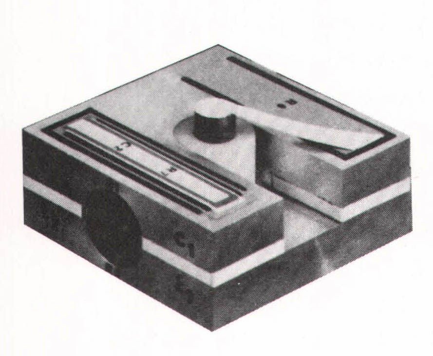
As a general description of the modern integrated circuit (IC), Dummer’s vision was astonishingly close to the mark. But the technical problems were formidable, and he had little idea of how to solve them. If many transistors were integrated into the same piece of semiconductor, how would they be isolated from each other electrically, so that the operation of one didn’t short-circuit the workings of another? A current dispatched to one transistor would spread throughout the device unless an electrical or physical barrier of some kind stopped it. But what kind? And how would resistors, capacitors, and other passive components, then made out of nonsemiconducting materials, be fashioned out of semiconductors? (Passive parts don’t amplify or otherwise change a current’s power.) Finally, how would the components be wired together, so that their operation could be coordinated? If they had to be wired by hand, then a solid circuit (the term integrated circuit didn’t come into use until the late 1950s) might be no less expensive or easier to make than discretes, and its performance no more reliable.
Back in England, Dummer attempted to put his ideas into practice. He prodded the Royal Radar Establishment to award a modest research and development contract to the Plessey Company in April 1957, but nothing came of Plessey’s work. “Dummer,” recalled a colleague, “was preaching the gospel of integrated circuitry long before anybody, including Dummer, had the slightest idea how you could actually do this…[Dummer] carried inspiration around on his back like pollen…He never received the backing that his degree of inspiration would have justified.” At another symposium, this time at Malvern in September 1957, Dummer and Plessey displayed a crude, inoperable model of an IC. It got a good deal of attention – from visiting Americans. But the Royal Radar Establishment was unconvinced and the contract was not renewed.
The climate on the other side of the Atlantic was much more receptive to miniaturization schemes, no matter how farfetched. The Defense Department was spending millions of dollars on research programs to make electronic components smaller, more reliable, less expensive, and easier to build. These efforts amounted to a sizable industry and reflected the military’s growing interest in electronic technology, which first became a major military concern during World War II, when all kinds of weapons contained electronic equipment; even that lumbering giant of the air, the B-29 bomber, was crammed with nearly a thousand vacuum tubes. The success of the next generation of weapons guided missiles, H-bombs, early-warning radar, computers – obviously depended on the state of electronics technology.
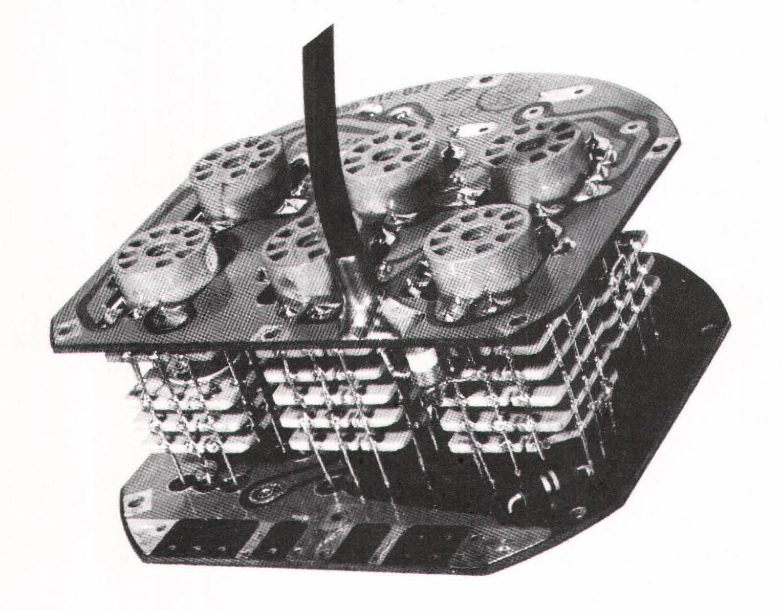
Each of the military services had a favored miniaturization plan. “Project Tinkertoy” was the earliest effort, begun in secret in 1950 by the National Bureau of Standards on behalf of the Navy. Tinkertoy was dedicated not so much to miniaturization as to automation and standardization. The project’s whimsical name derived from that popular wooden toy – the one with sticks and wheels that can be put together in almost any configuration – and was motivated by the same basic idea; the goal was to develop compact electronic modules, or subassemblies, composed of standardized discretes. If a set of modules for one project called for, say, five amplifiers, ten resistors, and twenty capacitors, the assembly line would gear up accordingly and the desired modules would be assembled automatically.
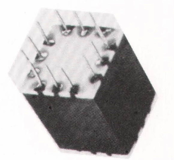
In principle, Tinkertoy was a good idea. But Tinkertoy didn’t get far, at least in its first incarnation. When the project was made public in 1953, it turned out that the entire scheme had been based on tubes instead of transistors, which had been invented more than five years earlier and would have made the modules much smaller and more reliable. With one foot in the future and another firmly in the past, Tinkertoy’s engineers had ignored one of the important inventions of the century. The project was cancelled in 1953, after the Navy had doled out almost $5 million in research and development funds.
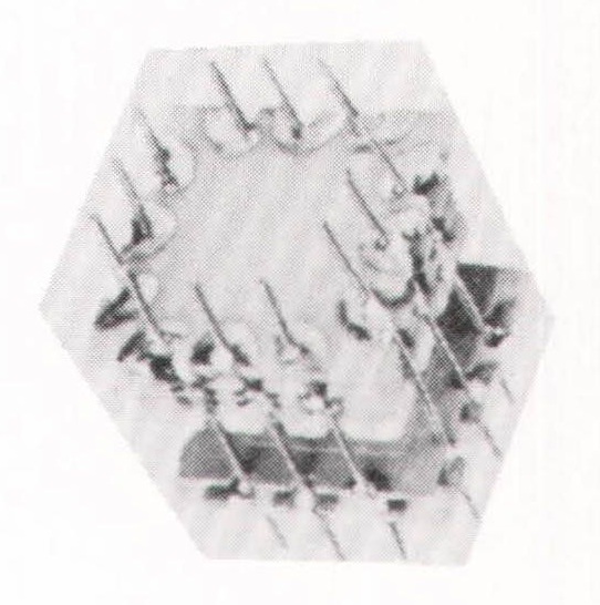
Yet the need for better components remained, and Tinkertoy was resurrected four years later, this time using transistors. The project had a new sponsor, the Army Signal Corps; a new general contractor, RCA; a new name, the Micromodule Plan; and a new triad of priorities, emphasizing miniaturization as much as automation and standardization. Otherwise, the basic idea was the same. In this case, transistors, resistors, and other components were deposited on tiny, standardized ceramic wafers about the diameter of a pencil; the wafers were stacked together, linked with wires along the sides, and then plugged into circuit boards. Micromodules were much smaller and more practical than Tinkertoys, and the Army, pleased with RCA’s work, spent $26 million on micromodules by 1963. Unfortunately, history repeated itself. Just as the Tinkertoy project had been done in by the invention of the transistor, the Micromodule Plan was rendered obsolete by the invention of the IC.